

Last month, we asked you to reverse engineer a chip from nothing but its layout and teased a bigger challenge. Results and our favorite writeups are coming soon. In the meantime, here’s our next challenge!
This time, you’re designing the chip, and we’ll pay to fabricate our favorite designs! We’re particularly interested in projects with unique functionality, as well as those that demonstrate novel approaches to design and verification methodologies! Winners will receive a fabricated copy of their chip, mounted on a dev boards, so they can test their design in real silicon.
The challenge
Design an open-source, general-purpose protocol emulator ASIC.
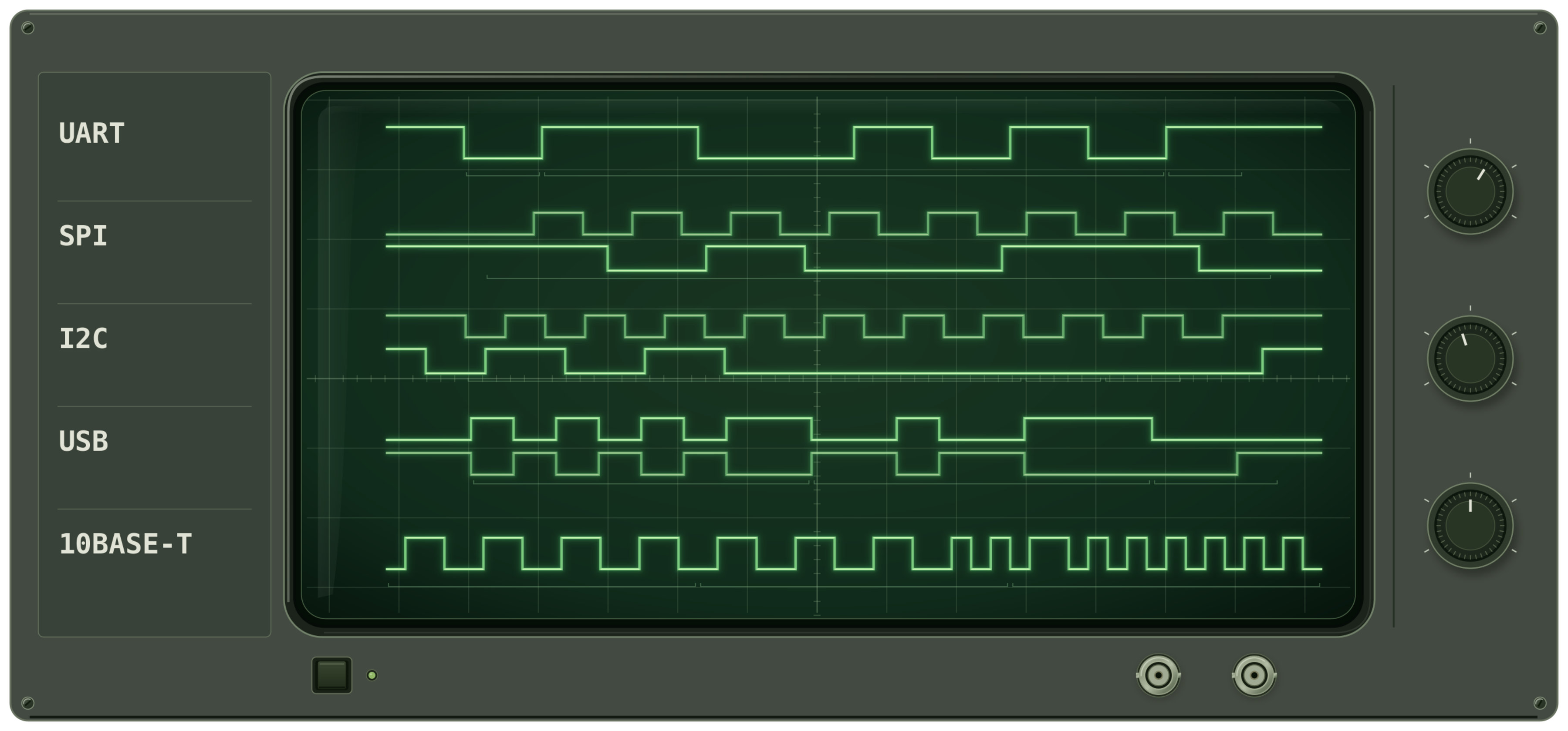
Hardware protocols like UART, SPI, and I2C are simple enough that people routinely “bit-bang” them: toggle pins from software with careful timing instead of using a dedicated peripheral. A protocol emulator is a small chip built to do exactly that: a tiny CPU with an instruction set designed for reading pins, writing pins, counting cycles, and hitting timing precisely enough that you can implement a real protocol in firmware rather than in fixed logic. Something like that is a useful tool for hardware debugging and reverse engineering, which is a good part of what we do.
The hard part is flexibility. The goal isn’t to put a UART block, an SPI block, and an I2C block on one die and call it done. Your chip should be reprogrammable enough to support new protocols after fabrication, within its timing and I/O constraints. For inspiration, look at the PIO state machines on the RP2040 or the PRU cores on TI’s Sitara parts, and consider what you’d do differently.
- Start with UART, SPI, and I2C.
- Stretch goals include low-speed USB and 10Mbit Ethernet.
- Other interesting protocols to consider: JTAG, SWD, PS/2, CAN bus
- If you have access to an FPGA, consider using it to test your RTL before the ASIC flow.
- Show us anything else your architecture makes possible that we haven’t thought of.
At Jane Street, we use Hardcaml to generate the RTL for our FPGA and ASIC designs. We are excited to see the languages and verification techniques you use, including formal methods, random constrained tests, AI-assisted verification, and more. As AI-assisted chip design becomes more common, we believe verification will be an extremely important aspect of the ASIC design flow going forwards.
The rules
- Process: We’re targeting IHP’s 130nm CMOS5L process through our friends at
Tiny Tapeout. Start with the CMOS5L Verilog
template, which
takes you from RTL to GDS. Set the tile size in
info.yamlto 6x4. - Area: The current maximum area is 6x4 tiles per design. We are working on the possibility of scaling up to 8x4 tiles (~30% more area). We’ll update this page, as well as emailing everyone who has signed up if the larger tile size becomes available.
- Open source: Your submission should be open source so others can use and build on it. Unlike the reverse-engineering puzzle, there’s no need to keep your work hidden until the deadline, so feel free to build in public!
- Teams: This is a much bigger project than the puzzle, so we strongly recommend working in teams.
- Deadline: Submit your design by January 18th, 2027.
- Prize: We’ll pay to tape out the most novel designs on a Tiny Tapeout shuttle. We’re targeting the March 2027 CMOS5L shuttle, subject to the foundry schedule. Winners will receive chips and dev boards back after fabrication, so you can test your design in silicon.
How much fits?
An 6x4 allocation is 24 tiles. At approximately 200um × 150um per tile, that’s about 0.7 mm² of nominal tile area. As a rough estimate, budget for about 1K logic cells per tile. You may need to get creative to fit the functionality you want.
For instruction memory, SRAM can be more area-efficient than flip-flops. Tiny Tapeout has examples of SRAM running on this process node you can reference.
Run synthesis early, check the mapped cell area, and leave room for clock-tree buffers and routing. Then run the full place-and-route flow and check timing. A design that looks small enough after synthesis can still be difficult to route or too slow at your chosen clock frequency.
Getting started
If you’ve never taped out a chip before, the Tiny Tapeout documentation walks through the process end to end, and the tools are all free and open source. Start by getting a UART transmitter out of a pin. Then make it programmable.
Sign-up If you’re interested, please fill out our sign-up form. We’ll send updates about the tapeout template, deadlines, as well as providing the final submission link. Note that filling out the form is not a commitment to participating, it’s just to receive updates!
We’ll add a final submission form to this page closer to the deadline!
If you have questions along the way, reach out to asic-competition@janestreet.com.
Hardware at Jane Street
The hardware team at Jane Street designs FPGAs and ASICs that run some of the fastest trading systems in the world. If designing a chip for fun sounds like your kind of thing, take a look at our hardware internships and full-time roles. You can also explore Hardcaml, our open-source OCaml hardware design libraries, or stay in touch.